Semiconductor manufacturing is built on processes that push materials to their limits. Tools must tolerate high-energy plasma, corrosive halogen gases, rapid temperature swings, and constant mechanical wear. When materials fail under these conditions, they introduce particles, drift in dimensional accuracy, and ultimately reduce yield.
As geometries shrink and tolerance windows tighten, engineers are turning more often to high purity alumina (HPA) because it provides the combination of purity, hardness, thermal stability, and plasma resistance that modern semiconductor equipment requires.
Why Semiconductor Equipment Needs Better Materials
Etching, deposition, and lithography steps all expose equipment surfaces to harsh chemistries and high temperatures. Fluorine-based plasmas, chlorine ions, and oxygen radicals aggressively attack most conventional ceramics and quartz. At the same time, front-end modules run at temperatures well above 1000 °C, while wafer-handling tools experience constant friction. These stresses cause surface erosion, cracking, chemical attack, and particle generation—failure modes that quickly undermine process control.
Ceramics that succeed in these environments share a few traits: they resist plasma, maintain dimensional stability at elevated temperatures, minimize contamination, and remain electrically insulating under RF fields. High purity alumina checks all of these boxes, which is why its adoption across semiconductor equipment has accelerated.
What Makes High Purity Alumina Effective
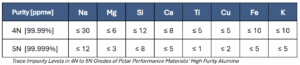
The defining characteristic of HPA is its exceptionally low impurity content. Metallic contaminants such as iron, copper, sodium, or chromium can migrate into wafers or create “killer defects” that destroy device yield. By contrast, 4N (99.99%) and 5N (99.999%) alumina from Polar Performance Materials is engineered for extremely low trace element levels and a consistent, tightly controlled particle size distribution. This results in dense, uniform ceramics with few pathways for chemical attack.
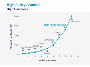
The α-phase crystal structure further strengthens resistance to fluorine and chlorine plasmas. Combined with the material’s high hardness—nearly the top of the Mohs scale—HPA withstands both plasma erosion and mechanical wear better than lower-purity alumina or quartz. Its thermal stability, with a melting point near 2050 °C, makes it especially suitable for components that undergo rapid heating and cooling.
Where HPA Is Used in Semiconductor Equipment
To understand why HPA is widely adopted, it helps to look at the specific components where it appears—and the operating conditions each one faces.
Wafer Chucks (Vacuum and Electrostatic)
A wafer chuck is the precision platform that holds a wafer during lithography, etching, CVD, and other front-end steps. Vacuum chucks use a network of micro-holes to secure the wafer with negative pressure, while electrostatic chucks (ESCs) rely on electrostatic forces. Both types must maintain flatness and withstand thermal excursions that often exceed 1000 °C. HPA’s thermal conductivity, dielectric strength, purity, and wear resistance make it an ideal material for the ceramic surfaces in these chucks.
Plasma Chamber Liners and Gas Distribution Plates
Inside a plasma etch chamber, the liner protects the chamber body and maintains a stable environment, while the gas distribution plate (or “showerhead”) disperses reactive gases uniformly over the wafer. These parts face the harshest chemistries in the fab, including fluorine-rich plasmas that rapidly corrode most materials. HPA’s dense microstructure and strong chemical resistance prevent fluorine penetration and limit erosion, maintaining chamber integrity and reducing particle generation.
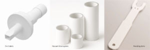
Die Collets
After wafers are diced, die collets pick up individual dies and place them on lead frames or substrates during assembly. This is a high-precision, high-speed operation where even small dimensional changes or surface wear can cause placement errors. HPA is commonly used for collets because it remains dimensionally stable, resists abrasion, and stays chemically clean during thousands of cycles.
Handling Arms and End Effectors
Handling arms move wafers between modules without direct human contact. Their end effectors must maintain cleanliness, avoid scratching the wafer, and perform reliably in vacuum or inert atmospheres. HPA’s hardness, chemical inertness, and very low particle generation make it a strong choice for these parts, especially in environments where contamination control is critical.
Other Components: Vacuum Interrupter Tubes
In high-voltage switching systems used throughout semiconductor equipment, HPA provides the dielectric strength and vacuum stability required to insulate internal electrodes and maintain long-term reliability.
Recommendations for Semiconductor Engineering
For engineers evaluating materials in semiconductor equipment, a few points stand out clearly:
- HPA extends component lifetime in plasma environments thanks to its α-phase structure and dense micro-architecture, which make it far more resistant to fluorine and chlorine attack than lower-grade ceramics.
- Ultra-high purity matters. The jump from standard alumina to 4N–5N grades reduces metallic contamination and helps prevent the microscopic defects responsible for a majority of yield loss.
- Thermal and dimensional stability are major advantages, especially for wafer chucks, ESCs, and components exposed to rapid heating and cooling.
- For mechanically active parts like collets and handling arms, HPA’s hardness limits abrasion and minimizes particle generation, directly improving process cleanliness.
Yield loss often traces back to microscopic contamination, drift in chamber conditions, or premature component wear. High purity alumina addresses all three. For fabs and OEMs aiming to safeguard yield and extend equipment life, it stands out as a material choice that pays for itself quickly.