Bulk crystal growth methods include:
- Kyropoulos (KY), top seeded crystal growth method utilizing large crucibles to grow very large sapphire boules of high quality
- Heat Exchange (HEM), bottom-seeded crystal growth method to grow high quality, uniform sized boules of high quality
- HDSM – Horizontal Direction solidification systems are used to produce large rectangular crystals for high quality window applications
- Czochralski (CZ) Ingot-style crystal growth method used to grow very high quality sapphire for small and medium diameter window and optical applications
The Polar Advantage
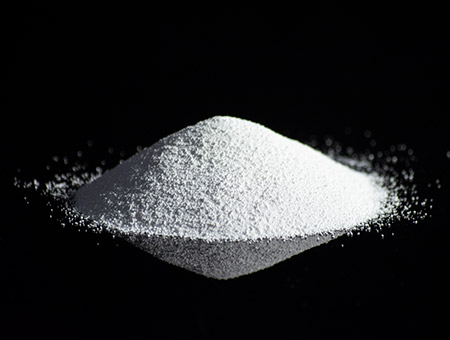
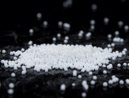
Higher Density Pellets
We press and sinter Polar 5N pellets in a continuous process that provides higher density pellets with very consistent density, shape, and purity to reduce micro bubbles and improve sapphire yields
Consistently Higher Purity
Reduced contaminants and strict process control deliver HPA pellets with higher and consistent purity helping improve sapphire crystal clarity and growth process repeatability
Better Packing Factor
High density HPA pellets maximize the amount of HPA in the crucible producing larger high-quality crystals per run and increasing throughput per furnace
Alumina Pellets Data Sheet
Request a Quote
5N Chemical Properties
| Elements | Concentration (ppmw) |
|---|---|
| Na | <3 |
| Mg | <1 |
| Si | <2 |
| Ca | <2 |
| Ti | <0.5 |
| Ga | <0.1 |
| Fe | <1 |
| Zn | <0.5 |
| K | <1 |
| Others | <0.5 |
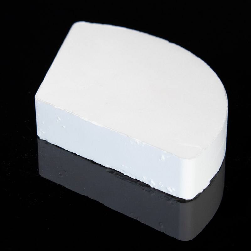
Physical Properties
| Property | ||||
|---|---|---|---|---|
| Shape | Square | Square | Wedge | Wedge |
| Fired Density (g/cm3) | 3.4-3.6 | 3.4-3.6 | 3.3-3.6 | 3.3-3.6 |
| Dimension (mm) | 40x40x20 | 55x55x40 | R90, 120o, H40 | R90, 90o, H40 |
| Weight (g) | 100-150 | 370-550 | 500-650 | 750-950 |
Applications
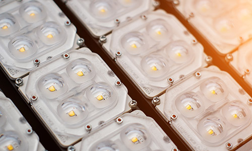
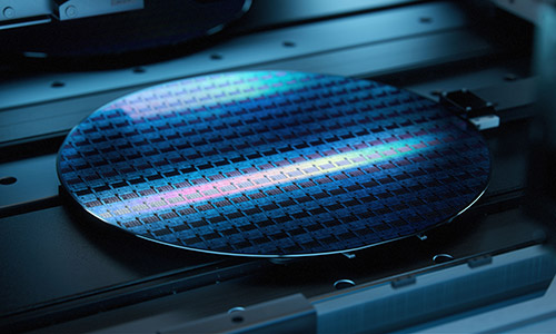
Sapphire Substrates
100mm to 200mm wafers for LEDs and MicroLEDs
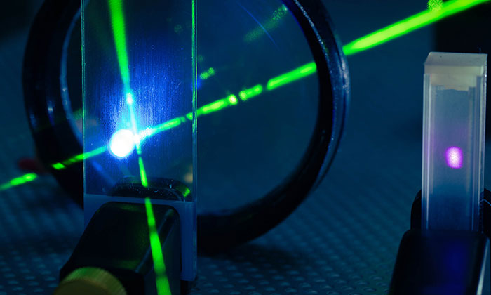
Optical Components
Windows and lenses for defense, aerospace, laser and oil field applications
Semiconductors
Sapphire wafers and components for CMOS and other chip processing
Other Pellet Applications include: Medical Device Components and Analytical Process Labware, Smartphone Screens, Camera Lenses